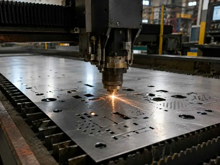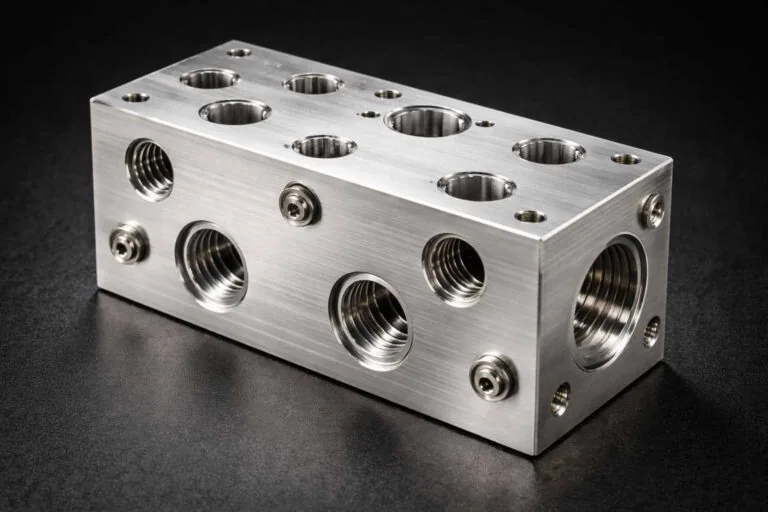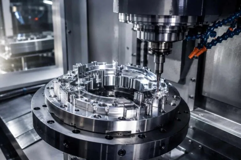
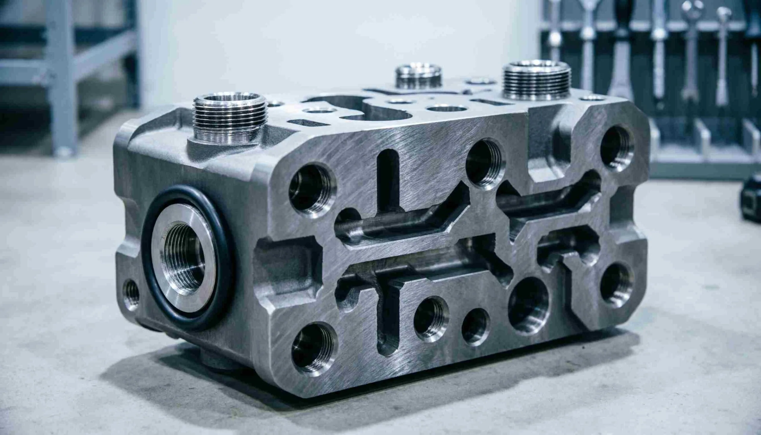
Semiconductor equipment parts are judged by what they leave behind. A chamber lid can be dimensionally perfect and still fail if it traps a pocket of air, sheds particles or outgasses under vacuum. Semiconductor machining therefore combines ordinary precision milling and turning with rules most industrial parts never meet: vacuum-safe geometry, controlled surface finish, compatible materials, precision cleaning and clean packing. This guide explains those rules for the machined parts that go into wafer processing, handling and inspection tools.
Key takeaways
- Most semiconductor equipment parts are aluminium 6061-T6, 316L stainless steel or engineering polymers such as PEEK. Zinc-bearing alloys such as brass are avoided in vacuum.
- Trapped volumes behind screws and in blind holes cause virtual leaks. Vented screws and through-holes are the standard fix.
- O-ring sealing faces need a controlled finish, typically Ra 0.4 to 0.8 µm with no radial scratches.
- Wetted stainless surfaces in gas delivery are specified under SEMI F19, and clean packing is referenced to cleanroom classes in ISO 14644-1.
- MW+ machines these parts with ±0.01mm to ISO 2768-m as the general tolerance, ±0.005mm on precision features and a finish ladder from Ra 3.2 µm to Ra 0.1 µm.
What counts as a semiconductor equipment part?
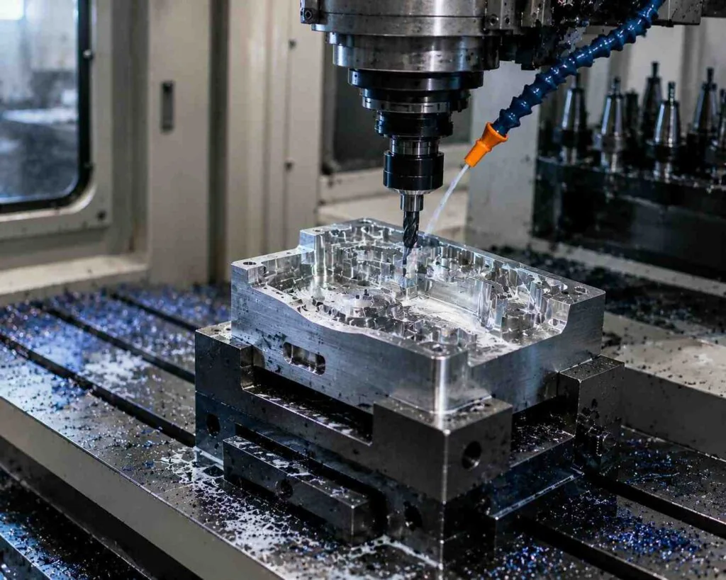
A wafer fab tool is a machine made of machines: a vacuum chamber where the process happens, a gas system that feeds it, a robot that moves wafers in and out, and a frame and enclosure that hold everything together. Each subsystem uses machined parts with different priorities.
| Subsystem | Typical machined parts | What matters most |
|---|---|---|
| Process chamber | Chamber bodies, lids, liners, gas distribution plates, pedestal parts | Vacuum integrity, sealing faces, surface finish, cleanliness |
| Gas delivery | Gas blocks, surface-mount substrates, fittings | Wetted-surface finish, internal cleanliness, leak tightness |
| Wafer handling | End effectors, robot arms, aligner parts | Flatness, low weight, contact materials that do not mark wafers |
| Vacuum hardware | Flanges, adapters, feedthrough housings | Sealing geometry and leak rate |
| Metrology and inspection | Stages, mounts, sensor brackets | Dimensional stability and thermal behaviour |
| Frames and enclosures | Brackets, covers, panels | Fit and finish, often sheet metal |
Which materials are used in semiconductor machining?
In semiconductor machining, material choice starts with the environment the part will see: vacuum, plasma, process gases, heat and contact with wafers. The table covers the common machined materials.
| Material | Typical parts | Why it is used | Machining note |
|---|---|---|---|
| Aluminium 6061-T6 | Chambers, lids, liners, handling parts | Light, stable, low outgassing once finished, anodisable | Fast to machine; distortion control on large plates |
| Stainless steel 316L | Gas blocks, fittings, vacuum flanges | Corrosion resistance, electropolishes well, weldable | Work-hardens; burr control inside ports |
| PEEK | Insulators, wafer contact pads, clamps | Clean, stable, chemically resistant | Large thermal expansion, measure at 20 °C |
| Polyetherimide (PEI) | Insulators, fixtures | Rigid, flame-resistant, good dielectric | Sharp tools, low heat |
| Polyimide (PI) | High-temperature insulators | Very high temperature capability | Expensive stock, careful handling |
| Invar and low-expansion alloys | Metrology mounts | Very low thermal expansion | Gummy, slow to machine |
Some materials are avoided outright. Brass and other zinc-bearing alloys release zinc under vacuum and heat, cadmium plating is excluded for the same reason, and porous castings trap gas and cleaning fluids. Ceramic parts such as alumina insulators are usually ground rather than milled and are made by ceramic specialists.
For the PEEK side of the list, our PEEK medical parts case study covers the same contamination and thermal problems in a medical setting.
Designing vacuum chamber parts that machine well
A vacuum chamber is only as good as its worst seal and its worst hidden cavity. Several machining details decide how quickly a chamber pumps down and whether it holds its base pressure.
| Feature | Problem | Rule |
|---|---|---|
| Screw in a blind tapped hole | Trapped gas leaks out slowly, a virtual leak | Vented screws, or a vent hole drilled to the bottom of the tapped hole |
| Mating surfaces clamped flat together | Gas trapped between the faces | Vent grooves or relief so the gap can pump out |
| O-ring groove | Leaks from scratches or poor finish | Ra 0.4–0.8 µm on the sealing surfaces, lay running round the groove, no radial marks |
| Knife-edge metal seal flange | A damaged edge will not seal | Protect the edge through every later operation and in packing |
| Internal corners and pockets | Places where contamination collects | Radii that clean easily, no crevices |
| Weld preparations | Porosity and trapped volumes at joints | Joint designs that weld from the vacuum side |
Leak tightness is usually proven with a helium leak test, and chamber and flange drawings often specify a maximum leak rate. That test catches real leaks. It does not catch virtual leaks, which is why trapped volumes have to be designed out rather than tested out.
For vacuum chamber bodies and lids, the practical sequence is to agree the seal type and groove standard first, then the venting of every tapped hole, then the finish on each sealing face. Settling those three points before the first cut avoids most of the rework we see on vacuum chamber parts drawn without a machinist’s input.
Surface finish and treatments
Surface finish in a vacuum chamber is not cosmetic. A rougher surface has more real area to adsorb water and gas, which slows pump-down, and a torn or smeared surface can shed particles. Gas-path surfaces are specified more tightly still.
| Treatment | Where it is used | Purpose |
|---|---|---|
| Fine-machined finish | Sealing faces, datum faces | Reliable sealing, stable measurement |
| Hard anodising (Type III) | Aluminium chamber parts exposed to plasma or wear | Wear and chemical resistance, electrical insulation |
| Electropolishing | Stainless steel gas-path components | Smooth, passive, low-particle wetted surfaces per SEMI F19 |
| Passivation | Stainless steel parts | Restores the chromium oxide layer, per ASTM A967 |
| Bead blasting | Chamber liners and shields | Controlled texture so deposits adhere rather than flake |
| Electroless nickel | Aluminium and steel parts needing hardness or solderability | Uniform coating on complex shapes |
Our finish ladder runs from Ra 3.2 µm as-machined to Ra 0.4 µm fine-machined and Ra 0.1 µm polished. The CNC surface finish chart explains the values, and how to specify Ra on a drawing covers the common mistakes.
Worked example: temperature and large aluminium plates
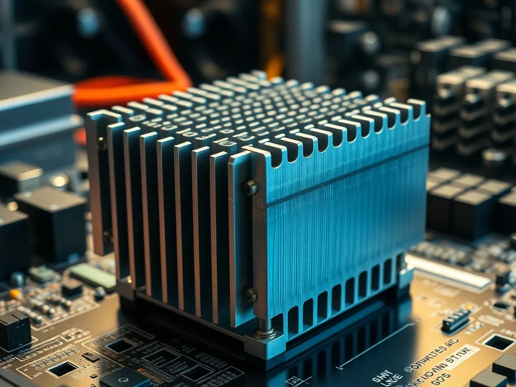
Chamber lids, base plates and gas distribution plates are often large, flat aluminium parts, and aluminium 6061 expands at about 23.6 µm per metre per kelvin. Temperature affects them twice.
- At inspection. A 300mm plate measured at 23 °C instead of the 20 °C reference grows by 300 × 23.6 × 3 = 21 µm. That is larger than a ±0.01mm tolerance band. Large aluminium parts must be soaked to temperature before they are measured.
- In service. A 400mm lid heated 60 K above room temperature during processing grows by 400 × 23.6 × 60 = 0.57mm. If it is bolted to a steel frame, which grows about half as much, the bolt holes and locating features must allow for the difference or the lid will bow.
Both numbers are easy to calculate and easy to forget. A supplier who raises them in the DFM review is one who understands where semiconductor equipment parts are going to be used.
Wafer handling parts: flatness, weight and contact
Wafer handling parts move a 300mm wafer worth more than the robot that carries it, so they are designed around three demands that pull against each other. They must be flat, so the wafer sits level and vacuum pads seal. They must be light, so the robot can move quickly without vibration. And any surface that touches the wafer must not scratch, contaminate or charge it.
| Requirement | Typical design response | Machining consequence |
|---|---|---|
| Flatness of the wafer support | Stress-relieved plate, symmetric pockets | Rough, release and finish, with light clamping on the final passes |
| Low weight | Deep lightening pockets, thin ribs | Thin-wall strategies and careful fixturing to avoid chatter |
| Non-marking wafer contact | PEEK or other polymer pads, defined contact points | Polymer parts machined and measured separately, then fitted |
| Vacuum grip | Small internal channels to suction pads | Drilled or milled channels, deburred and flushed clean |
| Static control | Conductive or dissipative materials where specified | Material grade fixed on the drawing, no substitutions |
These are among the most demanding semiconductor equipment parts to make well, because every weight-saving pocket makes flatness harder to hold. The answer in semiconductor machining is the same as for thin-walled housings: remove most of the material first, let the part settle, then finish.
Precision cleaning and clean packing
Precision cleaning is the step that turns a machined part into a semiconductor part. Machining leaves oils, coolant residue, fine chips and fingerprints, and any of them can end up on a wafer. A typical sequence looks like this:
- Deburr and inspect, because cleaning cannot remove a burr that has not yet broken off.
- Degrease to remove cutting fluids and oils.
- Ultrasonic cleaning in deionised water with a suitable detergent, reaching into holes and threads.
- Rinsing in deionised water to remove detergent residue.
- Drying with filtered gas or in a clean oven, so no water spots remain.
- Double-bagging in clean, low-outgassing film, with the inner bag opened only in the customer’s controlled area.
Cleaning cannot fix what machining leaves behind. A burr that survives deburring may break free during ultrasonic cleaning and settle in a blind hole, and a smeared surface holds contamination that no rinse removes. That is why precision cleaning starts at the machine, with sharp tools, controlled coolant and clean handling, not at the washing line.
The level of cleanliness and the environment for packing are specified by the equipment maker, often with reference to cleanroom classes under ISO 14644-1. Send the cleaning and packing specification with the RFQ, because it affects both price and lead time.
Documentation and change control
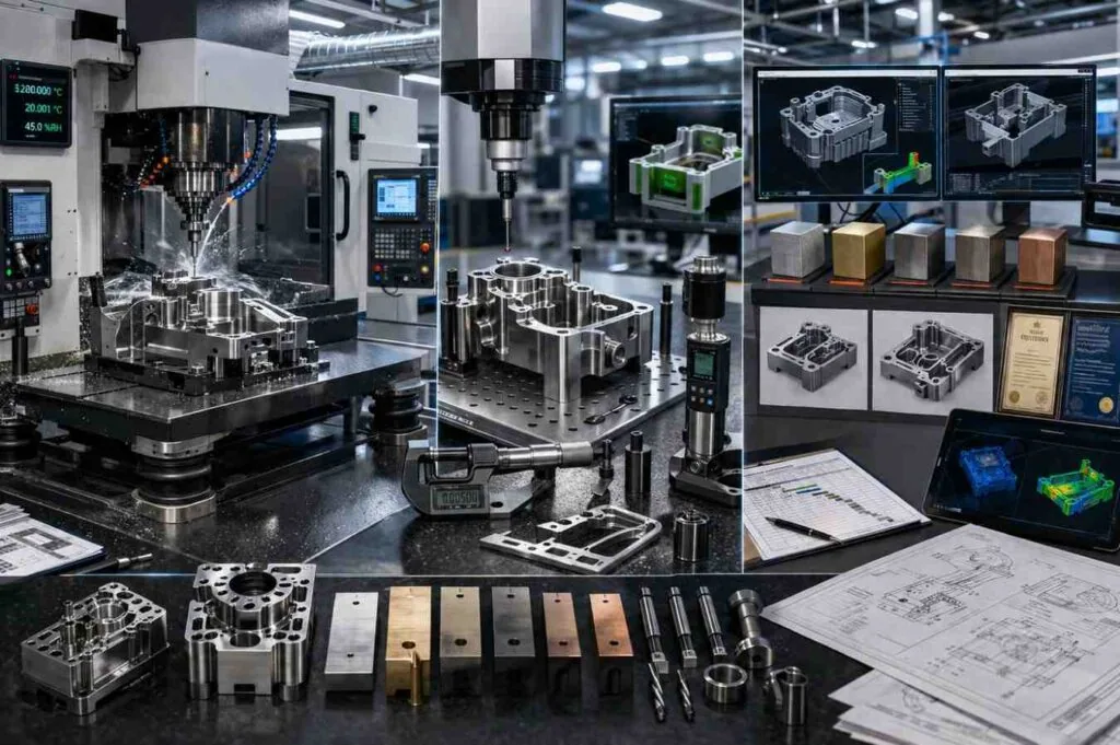
Equipment makers qualify a part once and then expect every later lot to be identical. That makes documentation and change control as important as the machining itself. For semiconductor equipment parts, the usual package is:
- A certificate of conformance for the lot, stating the drawing revision it was made to.
- A CMM inspection report on the characteristics the drawing marks as critical.
- Material certificates traceable to the heat or lot of stock.
- Records of finishing steps such as anodising, electropolishing or passivation.
- A record of the precision cleaning and packing performed, where the specification requires one.
Change control completes the picture. Equipment makers normally require notice before a supplier changes material source, finishing vendor, cleaning method or manufacturing location, because any of these can change outgassing or particle behaviour. At MW+, process changes on qualified parts are notified to the customer before they are used.
5 critical rules for machining semiconductor equipment parts
1. Design out trapped volumes
Every blind hole, clamped interface and hidden pocket is a potential virtual leak. Vent them at the design stage.
2. Specify finish by function
Give sealing faces, gas-path surfaces and cosmetic surfaces different finish requirements. One tight finish everywhere wastes money and time.
3. Keep materials vacuum-compatible
Name the exact alloy and polymer grade. Exclude zinc, cadmium and porous materials from anything that sees vacuum.
4. Control handling after cleaning
Once a part is cleaned, it should not be touched by bare hands, put on an uncovered bench or packed in ordinary film.
5. Inspect to the datums the tool uses
Measure parts against the features that locate them in the tool, at 20 °C, with a CMM programme that matches the drawing’s datum scheme. Our guide to the CMM inspection process explains why.
When a general CNC shop is the wrong supplier
Some parts of a semiconductor tool need specialist processes that sit outside a machining supplier’s scope. Being clear about that saves time.
- Ultra-high-purity gas weldments are made by specialists with orbital welding and dedicated cleanrooms. A machining supplier can make the machined fittings and blocks that go into them.
- Technical ceramics such as alumina and silicon carbide are ground and lapped by ceramic specialists.
- Coated consumables such as plasma-sprayed chamber parts are usually refurbished by coating specialists, with new base parts supplied by the machinist.
How MW+ supports semiconductor machining
MW+ is a precision CNC machining company in Shenzhen that machines aluminium, stainless steel and polymer CNC precision parts for equipment makers, from prototypes to production.
- CNC milling services on 3, 4 and 5-axis machines for chambers, plates, blocks and handling parts.
- Micro machining for small holes, fine slots and delicate features.
- Electrical discharge machining for sharp internal corners and hard materials.
- Every order ships with a certificate of conformance, a CMM report and material certificates.
For the aluminium side of the work, our guide to aluminium CNC milling covers alloys, tolerances and finishes in more depth.
Frequently asked questions
Which aluminium alloy is best for semiconductor chamber parts?
6061-T6 is the most common choice because it machines well, is dimensionally stable and anodises reliably. Some chamber designs use other wrought alloys for specific plasma or welding reasons. Machine to the grade the equipment maker specifies.
Can you machine vented screws and vent holes?
Yes. Vent holes to the bottom of tapped holes, vent grooves on mating faces and relief on clamped interfaces are routine. Show them on the drawing or ask us to flag trapped volumes in the DFM review.
What surface finish can you achieve on sealing faces?
Fine machining reaches Ra 0.4 µm, and polished surfaces reach Ra 0.1 µm. For O-ring faces we control both the Ra value and the direction of the machining lay, so marks run round the seal rather than across it.
Do you offer precision cleaning and double-bagging?
Final cleaning and double-bagging are planned to your specification. Send the cleaning and packing requirements with the RFQ so they are included in the route, price and lead time.
Can you machine PEEK and other polymer insulators?
Yes. PEEK, PEI and other engineering polymers are machined with sharp tools and measured at 20 °C, because polymers expand several times more than metals.
Do you helium leak test vacuum parts?
Tell us the leak-rate requirement and test method on the drawing, and we will confirm at quote stage how testing is handled for your part.
What tolerances do you hold on semiconductor equipment parts?
±0.01mm to ISO 2768-m generally, ±0.005mm on precision features and ±0.001mm on selected features. Flatness on large plates depends on size and stress relief, and we confirm it feature by feature.
Can you make both prototypes and production lots of semiconductor equipment parts?
Yes. Prototypes typically take 3 to 5 business days and production lots 10 to 15 business days, with the same programme, inspection plan and precision cleaning specification carried from the first part to the last. Qualified parts keep their process locked, and any change is notified before it is used.
What to send us
A STEP model, the drawing with sealing faces, finishes and treatments marked, the exact material grades, the cleaning and packing specification, and the quantities. You will get a quote and written DFM feedback within 24 hours, including a check for trapped volumes and finish requirements on your semiconductor equipment parts.