







RF connector impedance depends on the assembled transmission geometry and dielectric, not on a machined center pin alone. In an ideal uniform coaxial section, the inner-conductor diameter, outer-conductor inside diameter and intervening dielectric determine characteristic impedance. [1] A useful component review therefore starts with the complete interface, then assigns dimensions and inspection responsibilities to the center contact.
Illustrative application study: This guide is not a completed MW+ customer project or an RF qualification report. All dimensions, tolerances and dielectric values in the examples are assumed teaching inputs. The calculations use an ideal coaxial model and a rounded formula coefficient; they are not measured impedance, connector ratings or approved interface dimensions. A machined contact is a component of the assembly, not evidence that MW+ supplies or qualifies a complete RF connector.
Contents
Define the RF interface before the center contact
For the design review, identify the mating interface, nominal system impedance, operating band, cable or board transition and approved assembly definition. Name the RF design owner and the organization responsible for qualification. Keep those decisions separate from the machine shop’s component drawing and dimensional inspection scope.
Rosenberger’s SMA family is one documented example of a nominal 50 Ω connector family with a specified interface. [5] That does not make an arbitrary pin with a similar appearance an SMA contact or establish compatibility with the manufacturer’s product. Obtain the applicable interface drawing and exact mating requirements for the actual program.
Use a sectioned assembly model to identify the inner conductor, surrounding dielectric and inner surface of the outer conductor. Rohde & Schwarz describes those elements in its coaxial-cable explanation. [1] Label the axial region being reviewed so a local diameter calculation is not mistaken for an analysis of the entire connector.
Our recommended handoff package includes both component and assembly drawings. Mark which organization controls each dimension and dielectric feature. If the outer housing or insulator is supplied elsewhere, obtain its released requirements before assigning a center-pin tolerance. Record unresolved interface questions explicitly rather than making the machining supplier choose electrical design inputs.
RF connector impedance: use the coaxial model carefully
For an ideal concentric, uniform, nonmagnetic coaxial line, use the familiar low-loss relation Z₀ ≈ (60/√εᵣ) ln(D/d) Ω. Here d is the outside diameter of the inner conductor, D is the inside diameter of the outer conductor, and εᵣ is the relative permittivity of a uniform dielectric filling the region. WENSHING publishes this relation and its inverse; the coefficient 60 is a rounded engineering approximation. [2]
Both diameters must use the same unit so D/d is dimensionless. The logarithm is natural logarithm, ln, not base-10 logarithm. The output is characteristic impedance in ohms; it is not a prediction of the contact’s DC resistance. HUBER+SUHNER’s guide provides the transmission-line context and diameter definitions. [3]
Set the model boundary before using it. In the worked examples, the conductors are perfectly circular and concentric, the cross-section is constant, and the dielectric is homogeneous. The calculations omit losses, finite transitions, mating details, contact slots and local dielectric steps. Treat these as explicit omissions, not as features shown to have no effect.
HUBER+SUHNER discusses reflections associated with transmission-line discontinuities. [3] Our recommendation is to ask the RF designer which transitions require a fuller electromagnetic model and what evidence will validate the assembly. A uniform-section calculation can explain a dimensional relationship without qualifying a connector across its operating band.
Worked example: geometry and dielectric assumptions
Assume a target Z₀ of 50 Ω and an inner-conductor diameter d of 1.000 mm. Compare two purely assumed, constant dielectric values: εᵣ = 1.0 and εᵣ = 2.1. These are model inputs, not certified properties of a selected air space, polymer grade or manufactured insulator.
Rearranging the cited relation gives D/d = exp(Z₀√εᵣ/60), and therefore D = d × exp(Z₀√εᵣ/60). [2] The results below are original calculations using those assumptions. They describe the ideal uniform section only.
| Assumed relative permittivity εᵣ | Assumed d, mm | Target Z₀, Ω | Calculated D/d | Calculated D, mm |
|---|---|---|---|---|
| 1.0 | 1.000 | 50 | 2.300976 | 2.300976 |
| 2.1 | 1.000 | 50 | 3.345495 | 3.345495 |
For the first row, exp(50/60) = 2.30097589. Multiplying by the assumed 1.000 mm inner diameter gives D ≈ 2.300976 mm. In the second row, the assumed εᵣ changes the exponent, so the required ratio changes even though the target impedance and inner diameter remain the same.
The useful design question is whether the assembly model uses the actual dielectric arrangement. If the designer changes the insulator, do not keep the first row’s diameter ratio simply because it previously gave 50 Ω. Obtain applicable material data and decide how the real support geometry should enter the model. These two rows are not a material-selection recommendation.
Likewise, do not identify D from an unrelated outside measurement. In this calculation it is the outer conductor’s inner diameter in the modeled region, not the cable jacket diameter, connector nut diameter or insulator flange diameter. The actual drawing should make the controlled region unambiguous.
Worked example: diameter variation and model sensitivity
For a second exercise, fix εᵣ = 1.0 and choose rounded nominal dimensions d = 1.000 mm and D = 2.301 mm. Assume independent dimensional limits of d = 1.000 ±0.005 mm and D = 2.301 ±0.010 mm. These are invented intervals for sensitivity analysis, not recommended machining tolerances.
Within this mathematical model, increasing D raises ln(D/d), while increasing d lowers it. The minimum calculated impedance therefore uses the smallest D and largest d; the maximum uses the largest D and smallest d. The table evaluates those corners, with all other model inputs held fixed.
| Illustrative case | D, mm | d, mm | Calculated Z₀ = 60 ln(D/d), Ω |
|---|---|---|---|
| Rounded nominal dimensions | 2.301 | 1.000 | 50.001 |
| Lowest model value within assumed limits | 2.291 | 1.005 | 49.440 |
| Highest model value within assumed limits | 2.311 | 0.995 | 50.562 |
Check the lower corner directly: 60 × ln(2.291/1.005) = 49.4400517 Ω. The upper corner is 60 × ln(2.311/0.995) = 50.5615724 Ω. The rounded nominal dimensions produce approximately 50.000629 Ω, explaining the displayed 50.001 Ω rather than exactly 50 Ω.
No acceptance band has been assigned to the hypothetical assembly. Consequently, the range cannot be called passing or failing. It shows why the RF designer should assess combined variation before distributing component tolerances. A pin inspection report would address d; it would not independently establish the housing diameter, dielectric or assembled electrical response.
For a production review, ask which additional variations must be included and whether independent worst-case corners are physically relevant. Document the reasoning for any statistical approach or correlated dimensions. Do not present this simple bounding exercise as a production capability study or as proof of RF yield.
Translate the RF center contact into a machining drawing
Identify the modeled diameter and its controlled length
Mark the contact land represented by d and define its axial extent. Separate it from lead-ins, retention shoulders, termination features and other regions. Specify diameter and relevant geometric requirements on the released drawing. A nominal number taken from the model should not become an undocumented tolerance assignment.
Ask the RF designer and mechanical designer to agree the assembly references that locate the contact. Identify the inspected state and any constraints applied during measurement. If the component is intentionally flexible or includes slots, require a review of how the part is supported and evaluated. The uniform solid-cylinder example does not resolve those details.
Define the final condition after finishing
State whether the controlled diameter applies before or after the specified finish. Provide the approved material, temper, coating specification and controlled regions, with an explicit owner for any dimensional allowance. Do not infer a finish from image color or leave a coating change outside the interface review.
Keep electrical and dimensional responsibilities connected without treating them as identical. The manufacturing drawing defines the component to deliver; the RF design record explains how that component participates in the assembly. For broader pin-ordering information, the existing machined connector pin specification guide owns that general procurement topic.
Separate component inspection from RF validation
Prepare a component inspection plan against the released drawing. Identify the diameter region, controlled length, reference features and final condition. Agree a suitable measurement method and uncertainty treatment for each required result. Request actual values where appropriate and keep the drawing revision attached to the report.
For features that cannot be fully reached by the proposed instrument, require an explicit coverage review. Record what is measured directly, what is evaluated from other observations and what remains unverified. A convenient reading at one axial location should not silently become a report for the whole controlled region.
Assembly validation is a different record. Keysight describes VNAs as instruments that evaluate RF response using incident, reflected and transmitted signals, including magnitude and phase. It also explains that cables, connectors and fixtures affect results and that the calibration reference plane defines the measurement boundary. [4]
Our recommended RF test brief therefore names the complete device under test, mating hardware, frequency band, measured quantities, reference planes, calibration approach and acceptance criteria. Ask the test owner how adapters and fixtures are handled. Do not use the simple cable-identification procedure in reference [1] as a substitute for a connector’s approved qualification method.
Keep a clear link between the two records: component lot or sample identifier, assembly revision, configuration and test report. If a measured RF response is unacceptable, use that traceability to investigate the assembly and model rather than immediately assigning the cause to the pin diameter. This guide reports no physical RF test and makes no claim that MW+ owns a VNA or provides the described qualification service.
Release checklist and manufacturing next step
Before requesting a machining quote, resolve the following parallel requirements:
- Interface definition: Identify the actual connector family, mating drawing and approved assembly revision.
- Model scope: Mark the uniform section, input dimensions, dielectric assumptions and omitted transitions.
- Tolerance allocation: Review the pin together with the housing and insulator, rather than selecting a pin tolerance alone.
- Finished component: Define the controlled land, material, final finish stage and required geometry.
- Inspection: Agree measurement coverage, records and treatment of unresolved features.
- RF evidence: Assign the assembly-test owner and approved acceptance plan.
- Changes: Require the appropriate review when the mating component, dielectric, finish or controlled geometry changes.
Discuss the metal contact within MW+’s machined pin and connector-contact range. Once the interface requirements are defined, use its CNC manufacturing review to resolve component-production questions. Send MetalWorksPlus the released drawing and model, material and finish requirements, and the dimensional inspection scope. Confirm complete-assembly supply and RF testing separately if your program requires them.
Frequently asked questions
Is a 50 ohm connector simply a pin with 50 Ω resistance?
No. The discussion concerns the characteristic impedance of the transmission structure, which depends on its conductor geometry and dielectric. [1] [3] A pin’s DC resistance is a different quantity and does not establish the assembled RF interface.
Can the same center pin work with any surrounding dielectric?
Do not assume that it can. The ideal relation contains εᵣ as well as the diameter ratio. [2] The first table illustrates that dependence with assumed inputs; the actual dielectric arrangement and mating geometry need an application-specific review.
Does the 49.440–50.562 Ω example qualify a connector?
No. It is a calculated interval for an ideal uniform section using assumed diameter limits and fixed εᵣ. It provides no operating-band response, measured result or acceptance decision for a complete assembly.
What must an RF center contact inspection report show?
Our recommendation is to identify the drawing revision, controlled land, measured characteristics, final finish condition, measurement coverage and agreed acceptance basis. Keep that component report distinct from the assembled RF test record.
Can MW+ media prove the pictured contacts have RF performance?
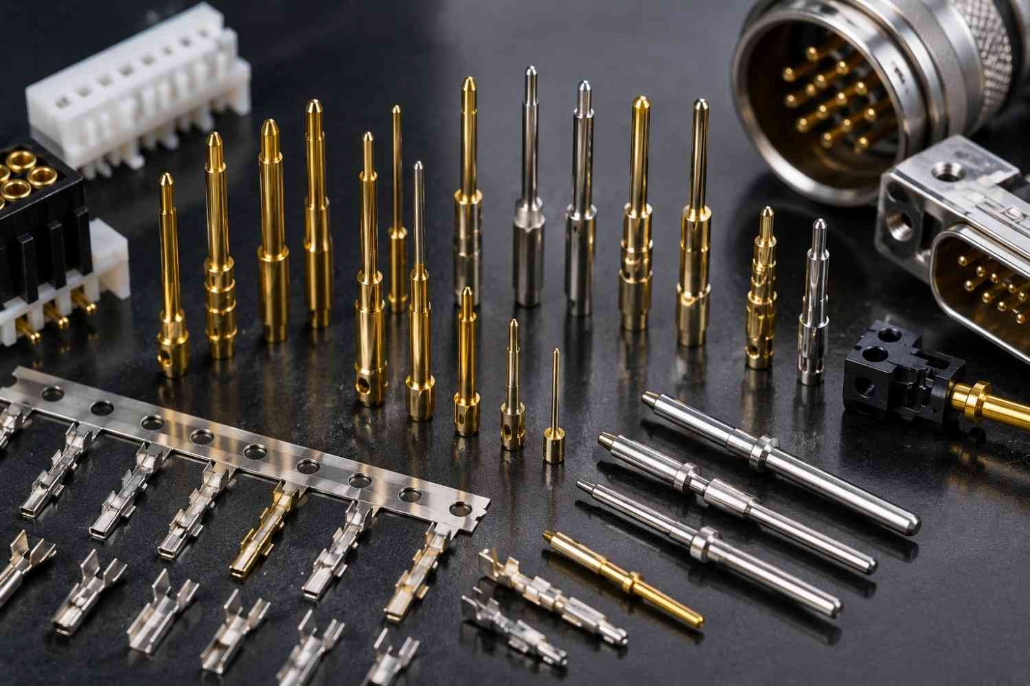
No qualification is inferred from these images. The library media provides component context only. Confirm the actual component supply scope and obtain application-specific RF evidence from the responsible assembly and test organizations.
Technical references
- Rohde & Schwarz: Cable Impedance Measurement. Coaxial conductor/dielectric structure; impedance depends on geometry and dielectric; cable measurement context, not a connector qualification recipe.
- WENSHING: Coaxial Line Impedance Calculator. Rounded 60/sqrt(epsilon_r) natural-log relation and inverse dimension ratio for ideal coax. Material presets are not adopted as actual material properties.
- HUBER+SUHNER: RF Connector Guide, fourth edition (2007), Sections 1.2–1.3. Historical technical reference for coaxial line definitions and discontinuities. No current catalog ratings or old standards adopted.
- Keysight: Network Analysis Fundamentals. VNA magnitude/phase, incident/reflected/transmitted signals and calibration reference-plane effects.
- Rosenberger: SMA Connector Family. Manufacturer-specific example of nominal 50-ohm impedance and an identified interface; no vendor ratings transferred to MW+.
Sources reviewed on 26 October 2026. The examples are original assumed-input calculations. Engineering review recommendations do not replace the governing interface drawing, RF design analysis or approved validation plan.